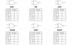
CUSTOM LAYOUT DESIGN (VLSI Custom Layout Design)

Custom Layout:

Layout Design starts normally with a schematic of the circuit layout and includes custom layout the use of EDA gear.

  • It is the back-end pastime of trendy cells/Analog IP which involves layout design of transistor-stage circuits.

  • As we all recognize, the again-quit layout of layout implementation known as an integrated circuit (IC) format -- is simplistically divided into ASIC-fashion float and full-custom go with the flow. This article will try to help customers define the numerous flavors of the whole-custom layout. The ideas offered here observe in popular. However, the examples and references proven refer in most cases to CMOS layout design. For a newcomer to VLSI layout, complete-custom go with the flowing manner polygon-degree format accomplished absolutely through the usage of easy polygon pusher software. A lot of people around the world carry out this feature and not unusual understanding says the only solution to increasing the quantity and velocity of format is to rent greater people. In fact, there are four wonderful flavors of complete-custom layout and each offers quite a number of opportunities for automation.

  1. Full-custom layout pushed by means of region obstacles or special software needs: This kind of layout is made of repeated complex systems like experience amplifiers, decoders, adders, multipliers in trendy, a datapath with tight control over the region, signal noise, bit symmetry. We seek advice from this form of layout as "datapath layout."
  2. Full-custom format to deal with high performance or analog circuitry design: This includes segment-locked loops (PLLs), digital-to-analog converters or analog-to- virtual converters (DACs/ADCs), electrostatic discharge (ESD) structures, regulators, radio frequency (RF) speed necessities, or techniques to fulfill low-energy wishes. Let's call this form of layout "analog layout."
  3. Full-custom layout that requires extra interest to location and overall performance than the entire digital (ASIC) go with the flow, however, has much less stringent requirements for pace and less want for control over device-degree layout than datapath or analog layout: We name this form of layout "custom virtual format."
  4. Full-custom layout for cell development: Cells are defined as logical building blocks that are part of a family of components that share common abutment rules, performance characteristics, or functionality. Examples would include the cells within a standard cell library or family of Pad cells. Let's call this type of layout "cell layout."

  • All 4 types of full-custom format are pushed by way of a schematic-based layout fashion as opposed to a language-primarily based design fashion which makes use of Verilog or VHDL (the basis for the ASIC design glide). Each of those complete-custom format categories ought to be used as had to gain the general necessities of the IC under improvement and, in popular, the tradeoffs between the layout styles middle-round area and performance considerations (see Figure 1). Let's look in extra element at each fashion, the thinking at the back of the technique, the design requirements and waft, the gear used for advent, and the preservation and migration between procedure technologies.

Comments

Popular posts from this blog

About "ICLabs"

"Digital Logic Gates"